 | ÐлекÑÑоннÑй компоненÑ: LTC2901 | СкаÑаÑÑ:  PDF PDF  ZIP ZIP |
Äîêóìåíòàöèÿ è îïèñàíèÿ www.docs.chipfind.ru
1
LTC2901
2901is sn2901
Programmable Quad Supply
Monitor with Adjustable Reset
and Watchdog Timers
June 2002
Information furnished by Linear Technology Corporation is believed to be accurate and reliable.
However, no responsibility is assumed for its use. Linear Technology Corporation makes no represen-
tation that the interconnection of its circuits as described herein will not infringe on existing patent rights.
s
Simultaneously Monitors Four Supplies
s
16 User Selectable Combinations of 5V, 3.3V, 3V,
2.5V, 1.8V, 1.5V and/or
±
Adjustable Voltage
Thresholds
s
Guaranteed Threshold Accuracy:
±
1.5% of
Monitored Voltage Over Temperature
s
Low Supply Current: 43
µ
A Typ
s
Adjustable Reset Time
s
Adjustable Watchdog Time
s
Open-Drain RST Output (LTC2901-1)
s
Push-Pull RST Output (LTC2901-2)
s
Individual Nondelayed Monitor Output for Each Supply
s
Power Supply Glitch Immunity
s
Guaranteed RST for V
CC
1V
The LTC
®
2901 is a programmable supply monitor for
systems with up to four supply voltages. One of 16 preset
or adjustable voltage monitor combinations can be se-
lected using an external resistor divider connected to the
program pin. The preset voltage thresholds are accurate
to 1.5% over temperature. All four voltage comparator
outputs are connected to separate pins for individual
supply monitoring.
The reset and watchdog delay times are adjustable using
external capacitors. Tight voltage threshold accuracy and
glitch immunity ensure reliable reset operation without
false triggering. The RST output is guaranteed to be in the
correct state for V
CC
down to 1V. The LTC2901-1 features
an open-drain RST output, while the LTC2901-2 has a
push-pull RST output.
The 43
µ
A supply current makes the LTC2901 ideal for
power conscious systems and it may be configured to
monitor less than four inputs. The parts are available in
the 16-lead narrow SSOP package.
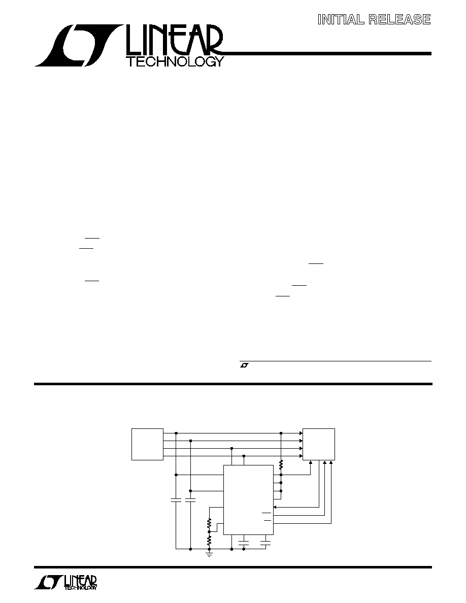
Quadruple Supply Monitor (5V, 3.3V, 2.5V, 1.8V)
s
Desktop and Notebook Computers
s
Multivoltage Systems
s
Telecom Equipment
s
Portable Battery-Powered Equipment
s
Network Servers
Final Electrical Specifications
FEATURES
DESCRIPTIO
U
APPLICATIO S
U
TYPICAL APPLICATIO
U
, LTC and LT are registered trademarks of Linear Technology Corporation.
V1
V2
V
REF
V
PG
COMP1
COMP2
COMP3
COMP4
WDI
WDO
RST
GND
10
11
R1
59k
1%
R3
10k
POWER
GOOD
R2
40.2k
1%
12
6
7
8
15
1
16
2
13
3
14
4
9
5
C
WT
47nF
C
RT
47nF
C2
0.1
µ
F
C1
0.1
µ
F
V4
V3
LTC2901-2
CWT
CRT
t
RST
= 216ms
t
WD
= 940ms
2901 TA01
DC/DC
CONVERTER
1.8V
2.5V
3.3V
5V
SYSTEM
LOGIC
2
LTC2901
2901is sn2901
SYMBOL
PARAMETER
CONDITIONS
MIN
TYP
MAX
UNITS
V
RT50
5V, 5% Reset Threshold
V1 Input Threshold
q
4.600
4.675
4.750
V
V
RT33
3.3V, 5% Reset Threshold
V1, V2 Input Threshold
q
3.036
3.086
3.135
V
V
RT30
3V, 5% Reset Threshold
V2 Input Threshold
q
2.760
2.805
2.850
V
V
RT25
2.5V, 5% Reset Threshold
V2, V3 Input Threshold
q
2.300
2.338
2.375
V
V
RT18
1.8V, 5% Reset Threshold
V3, V4 Input Threshold
q
1.656
1.683
1.710
V
V
RT15
1.5V, 5% Reset Threshold
V3, V4 Input Threshold
q
1.380
1.403
1.425
V
V
RTA
ADJ Reset Threshold
V3, V4 Input Threshold
q
0.492
0.500
0.508
V
V
RTAN
ADJ Reset Threshold
V4 Input Threshold
q
18
0
18
mV
V
CC
Minimum Internal Operating Voltage
RST, COMPX in Correct Logic State;
q
1
V
V
CC
Rising Prior to Program
V
CCMINP
Minimum Required for Programming
V
CC
Rising
q
2.42
V
V
CCMINC
Minimum Required for Comparators
V
CC
Falling
q
2.32
V
V
REF
Reference Voltage
V
CC
2.3V, I
VREF
=
±
1mA, C
REF
1000pF
q
1.192
1.210
1.228
V
V
PG
Programming Voltage Range
V
CC
V
CCMINP
q
0
V
REF
V
I
VPG
V
PG
Input Current
V
PG
= V
REF
q
±
20
nA
I
V1
V1 Input Current
V1 = 5V, I
VREF
= 12
µ
A, (Note 4)
q
43
75
µ
A
I
V2
V2 Input Current
V2 = 3.3V
q
0.8
2
µ
A
I
V3
V3 Input Current
V3 = 2.5V
q
0.52
1.2
µ
A
V3 = 0.55V (ADJ Mode)
q
15
15
nA
I
V4
V4 Input Current
V4 = 1.8V
q
0.34
0.8
µ
A
V4 = 0.55V (ADJ Mode)
q
15
15
nA
V4 = 0.05V (ADJ Mode)
q
15
15
I
CRT(UP)
CRT Pull-Up Current
V
CRT
= 0V
q
1.4
2
2.6
µ
A
I
CRT(DN)
CRT Pull-Down Current
V
CRT
= 1.3V
q
10
20
30
µ
A
t
RST
Reset Time-Out Period
C
RT
= 1500pF
q
4.9
6.9
8.9
ms
ORDER PART
NUMBER
GN16 PART MARKING
29011
29012
29011I
29012I
T
JMAX
= 125
°
C,
JA
= 130
°
C/W
The
q
denotes the specifications which apply over the full operating
temperature range, otherwise specifications are at T
A
= 25
°
C. V
CC
= 5V, unless otherwise noted. (Note 3)
(Notes 1, 2, 3)
V1, V2, V3, V4, V
PG
..................................... 0.3V to 7V
RST (LTC2901-1)........................................ 0.3V to 7V
RST (LTC2901-2).......................... 0.3V to (V2 + 0.3V)
COMPX ....................................................... 0.3V to 7V
CWT, WDO .................................................. 0.3V to 7V
V
REF
, CRT, WDI ............................ 0.3V to (V
CC
+ 0.3V)
Reference Load Current (I
VREF
) ............................
±
1mA
V4 Input Current (ADJ Mode) ............................. 1mA
Operating Temperature Range
LTC2901-1C/LTC2901-2C ....................... 0
°
C to 70
°
C
LTC2901-1I/LTC2901-2I .................... 40
°
C to 85
°
C
Storage Temperature Range .................. 65
°
C to 150
°
C
Lead Temperature (Soldering, 10 sec)................... 300
°
C
LTC2901-1CGN
LTC2901-2CGN
LTC2901-1IGN
LTC2901-2IGN
ABSOLUTE AXI U RATI GS
W
W
W
U
PACKAGE/ORDER I FOR ATIO
U
U
W
Consult LTC Marketing for parts specified with wider operating temperature ranges.
ELECTRICAL CHARACTERISTICS
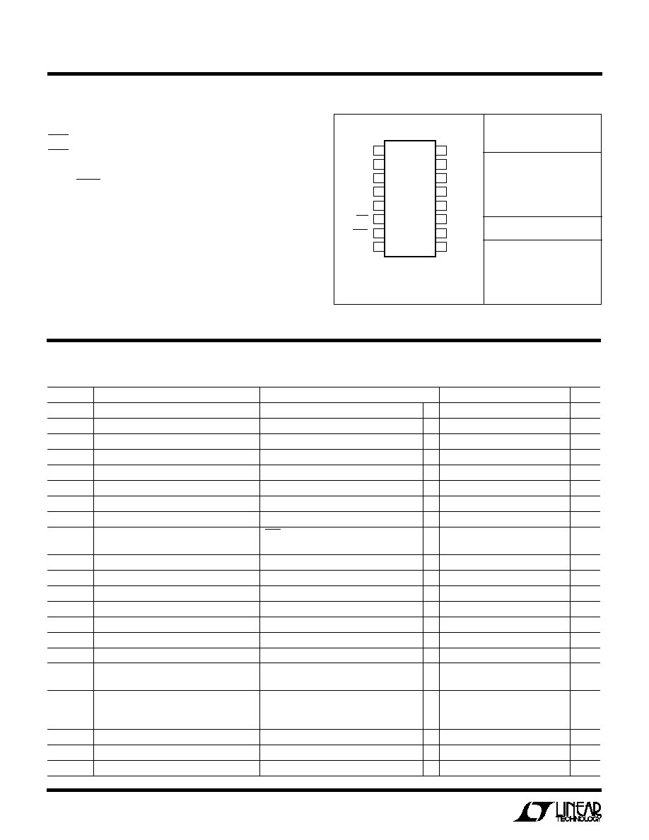
GN PACKAGE
16-LEAD PLASTIC SSOP
1
2
3
4
5
6
7
8
TOP VIEW
16
15
14
13
12
11
10
9
COMP3
COMP1
V3
V1
CRT
RST
WDO
WDI
COMP2
COMP4
V2
V4
V
REF
V
PG
GND
CWT
3
LTC2901
2901is sn2901
SYMBOL
PARAMETER
CONDITIONS
MIN
TYP
MAX
UNITS
t
UV
V
X
Undervoltage Detect to RST or COMPX
V
X
Less Than Reset Threshold V
RTX
150
µ
s
by More Than 1%
V
OL
Output Voltage Low RST, COMPX
I
SINK
= 2.5mA; V1 = 3V, V2 = 3V;
q
0.15
0.4
V
V3, V4 = 0V; V
PG
= 0V
I
SINK
= 100
µ
A; V2 = 1V; V1, V3, V4 = 0V
q
0.05
0.3
V
I
SINK
= 100
µ
A; V1 = 1V; V2, V3, V4 = 0V
q
0.05
0.3
V
V
OH
Output Voltage High RST, WDO, COMPX
I
SOURCE
= 1
µ
A
q
V2 1
V
(Note 5)
V
OL
Output Voltage Low WDO
I
SINK
= 2.5mA; V1 = 5V, V2 = 3.3V;
q
0.15
0.4
V
V3, V4 = 1V; V
PG
= 0V
V
OH
Output Voltage High RST (LTC2901-2)
I
SOURCE
= 200
µ
A
q
0.8 · V2
V
(Note 6)
I
CWT(UP)
CWT Pull-Up Current
V
CWT
= 0V
q
1.4
2
2.6
µ
A
I
CWT(DN)
CWT Pull-Down Current
V
CWT
= 1.3V
q
10
20
30
µ
A
t
WD
Watchdog Time-Out Period
C
WT
= 1500pF
q
20
30
40
ms
V
IH
WDI Input Threshold High
V
CC
= 3.3V to 5.5V
q
1.6
V
V
IL
WDI Input Threshold Low
V
CC
= 3.3V to 5.5V
q
0.4
V
t
WP
WDI Input Pulse Width
V
CC
= 3.3V
q
150
ns
I
WDI
WDI Pull-Up Current
V
WDI
= 0V
10
µ
A
The
q
denotes the specifications which apply over the full operating
temperature range, otherwise specifications are at T
A
= 25
°
C. V
CC
= 5V, unless otherwise noted. (Note 3)
ELECTRICAL CHARACTERISTICS
Note 1: Absolute Maximum Ratings are those values beyond which the life of
a device may be impaired.
Note 2: All voltage values are with respect to GND.
Note 3: The greater of V1, V2 is the internal supply voltage (V
CC
).
Note 4: Under static no-fault conditions, V1 will necessarily supply quiescent
current. If at any time V2 is larger than V1, V2 must be capable of supplying
the quiescent current, programming (transient) current and reference load
current.
Note 5: The output pins RST, WDO and COMPX have internal pull-ups to V2
of typically 6
µ
A. However, external pull-up resistors may be used when faster
rise times are required or for V
OH
voltages greater than V2.
Note 6: The push-pull RST output pin on the LTC2901-2 is
actively pulled up
to V2.
4
LTC2901
2901is sn2901
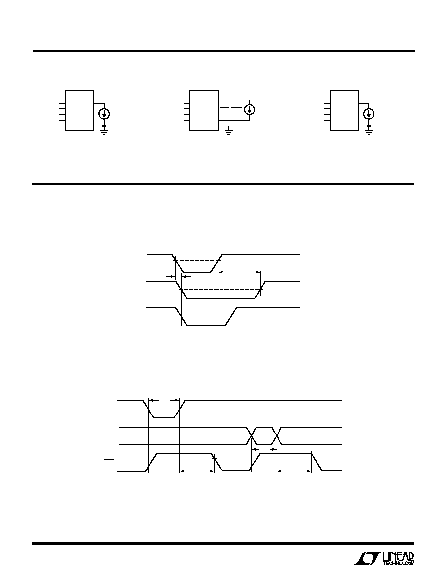
TI I G DIAGRA S
W
U
W
V
X
Monitor Timing
t
RST
2901 TD
V
RTX
V
X
RST
COMPX
t
UV
1.5V
Watchdog Timing
t
RST
t
WP
t
WD
t
WD
2901 TD2
RST
WDI
WDO
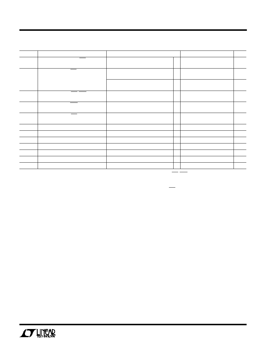
TEST CIRCUITS
Figure 1. RST, WDO, COMPX V
OH
Test
V1
V2
V3
V4
2901 F01
LTC2901-1
RST, WDO
OR COMPX
I
SOURCE
1
µ
A
Figure 2. RST, WDO, COMPX V
OL
Test
V1
V2
V3
V4
2901 F02
LTC2901-1
I
SINK
2.5mA,
100
µ
A
RST, WDO
OR COMPX
Figure 3. Active Pull-Up RST V
OH
Test
V1
V2
V3
V4
2901 F03
LTC2901-2
RST
I
SOURCE
200
µ
A
5
LTC2901
2901is sn2901
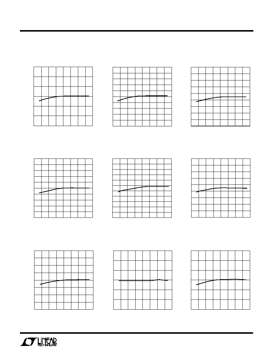
2.5V Threshold Voltage
vs Temperature
1.8V Threshold Voltage
vs Temperature
1.5V Threshold Voltage
vs Temperature
ADJ Threshold Voltage
vs Temperature
ADJ Threshold Voltage
vs Temperature
TEMPERATURE (
°
C)
60
THRESHOLD VOLTAGE, V
RT25
(V)
2.3750
2.3675
2.3600
2.3525
2.3450
2.3375
2.3300
2.3225
2.3150
2.3075
2.3000
20
20
40
2901 G04
40
0
60
80
100
TEMPERATURE (
°
C)
60
1.655
THRESHOLD VOLTAGE, V
RT18
(V)
1.665
1.675
1.685
1.695
20
20
60
100
2901 G05
1.705
1.710
1.660
1.670
1.680
1.690
1.700
40
0
40
80
TEMPERATURE (
°
C)
60
THRESHOLD VOLTAGE, V
RT15
(V)
1.425
1.420
1.415
1.410
1.405
1.400
1.395
1.390
1.385
1.380
20
20
40
2901 G06
40
0
60
80
100
TEMPERATURE (
°
C)
60
THRESHOLD VOLTAGE, V
RTA
(V)
0.508
0.506
0.504
0.502
0.500
0.498
0.496
0.494
0.492
20
20
40
2901 G07
40
0
60
80
100
TEMPERATURE (
°
C)
60
THRESHOLD VOLTAGE, V
RTAN
(V)
0.018
0.012
0.006
0
0.006
0.012
0.018
20
20
40
2901 G08
40
0
60
80
100
TYPICAL PERFOR A CE CHARACTERISTICS
U
W
5V Threshold Voltage
vs Temperature
3.3V Threshold Voltage
vs Temperature
3V Threshold Voltage
vs Temperature
TEMPERATURE (
°
C)
60
THESHOLD VOLTAGE, V
RT50
(V)
4.675
4.700
4.750
4.725
0
40
100
2901 G01
4.650
4.625
4.600
40 20
20
60
80
TEMPERATURE (
°
C)
60
THRESHOLD VOLTAGE, V
RT33
(V)
3.135
3.125
3.115
3.105
3.095
3.085
3.075
3.065
3.055
3.045
3.035
20
20
40
2901 G02
40
0
60
80
100
TEMPERATURE (
°
C)
60
THRESHOLD VOLTAGE, V
RT30
(V)
2.850
2.840
2.830
2.820
2.810
2.800
2.790
2.780
2.770
2.760
20
20
40
2901 G03
40
0
60
80
100
TEMPERATURE (
°
C)
60
V
REF
(V)
1.228
1.222
1.216
1.210
1.204
1.198
1.192
20
20
40
2901 G23
40
0
60
80
100
V
REF
vs Temperature